INNOVATION THROUGH CONSILIENCE
코팅공정, 트랜지스터 소자 성능 및 응용에 따라 다양한 유기 반도체 재료 선정
| Formulation | Coating Method | Mobility | |||
|---|---|---|---|---|---|
| Spin | Slot-die | Inkjet | Gravure | ||
| CP3100 | ● | ● | ● | ● | 0.5 ~ 1.0 |
| CP4100 | ● | ● | ● | ● | 0.3 ~ 0.6 |
| CP5100 | ● | ~ 4.0 | |||
| CN5100 | ● | ● | ● | ● | ~ 0.5 |
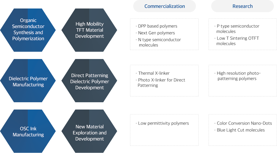
Planarization Layer A5XXX
CP3100 Series
ㆍEnable aSi replacement
ㆍMobility up to 1㎠/Vs
CP4100 Series
ㆍMobility up to 1㎠/Vs
ㆍCross-linkable semiconductor
CP5100 Series
ㆍMobility up to 4㎠/Vs
CN5000 Series
ㆍMobility up to 1.5㎠/Vs
CD2200 Series
ㆍThermally cross linking dielectric
CD7100 Series
ㆍUV photopatternable dielectric
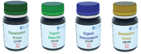
Inkset C1000SP
ㆍBased on CP3100
ㆍOptimized for spin coating
Inkset C2000SL
ㆍBased on CP5100
ㆍOptimized for slot die or blade coating of OSC
Inkset C3000S
ㆍInkset for Metal Layer
X-Ray Detector Fingerprint Sensor
X-Ray Detector
Display Backplanes OLED, Micro-LED
ㆍ다양한 코팅방식에 적합한 유기 p-type 반도체 재료
ㆍ균일한 소자 특성과 우수한 대기 안정성 보유
ㆍNon-halogenated 용매를 이용한 잉크 조액
ㆍBottom-gate와 Top-gate 트랜지스터 구조에 적합하게 적용 가능
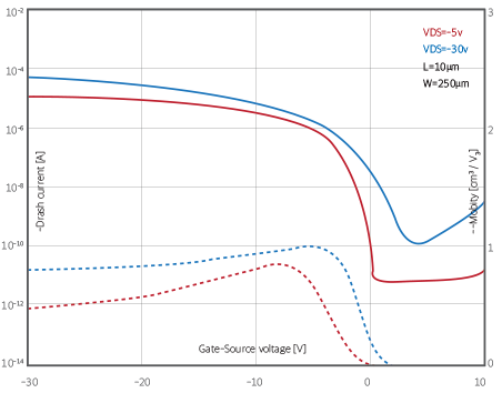
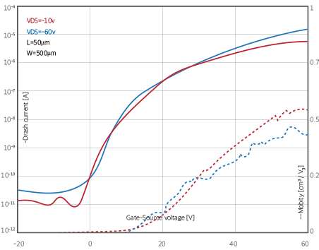
ㆍ이동도 0.5~1 cm2/Vs
ㆍOn/Off ratio > 106
ㆍa-Si 소자 성능을 저가 기재에서 구현 가능
| Method | Viscosity(mPas) | Availability | Applications |
|---|---|---|---|
| Spin-coating | 1.0 – 2.0 | ● |
EPD, LCD (display backplane) Logic Circuits, Sensors (in logistics, packaging, …) |
| Slot-die coating | 1.0 – 8.0 | ● | |
| Inkjet printing | ● | ||
| Gravure printing | ● | ||
| Stripe coating | 0.5 – 3.0 | ● | |
| Flexographic printing | ● |
ㆍ유기 반도체 조액과 소자의 우수한 공기 안정성 보유
ㆍNon-halogenated 용매를 이용한 잉크 조액
ㆍBottom-gate와 Top-gate 트랜지스터 구조에 적합하게 적용 가능
ㆍ이동도 ~0.5 cm2/Vs
ㆍPET 기재에 모든 공정이 가능
| Method | Viscosity(mPas) | Availability | Applications |
|---|---|---|---|
| Spin-coating | 0.5 – 1.5 | ● |
EPD, LCD (display backplane) Logic Circuits, Sensors (in logistics, packaging, …) |
| Slot-die coating | 1.0 – 8.0 | ● | |
| Inkjet printing | ● | ||
| Stripe coating | 0.5 – 3.0 | ● |
(주)클랩 / CLAP Co.,Ltd
서울시 강동구 천호대로 1006, 13층 1306호
대표_김성호 사업자등록번호_764-88-01246
Copyright (c) 2022 CLAP Co.,Ltd. All rights reserved.
E-mail_ johnny@clap.co.kr