INNOVATION THROUGH CONSILIENCE
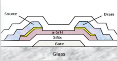
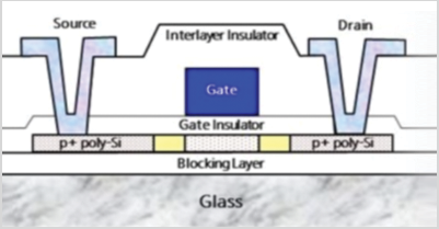
| Category | a-Si on Glass | LTPS on Plastic | OTFT on Film |
|---|---|---|---|
| Process Temp. | 300 °C | 250 °C | 100 °C |
| Process | CVD, Dry Etcher, PVD Sheet by Sheet process |
CVD, Dry Etcher, PVD Sheet by Sheet process |
Wet(Liquid) coating and development Roll to Roll process |
| No. of Mask | 4~5 | 7~11 | 4~5 |
| Mobility | 0.1 ~ 1.0 cm2/Vsec | 20 ~ 100 cm2/Vsec | 0.5 ~ 4 cm2/Vsec |
| Off Current(A) | >10-12 | 10-14~10-12 | >10-14 |
| Substrate | Glass | Soluble PI | PET, PEN, PI, Poly-ketone, PC etc |
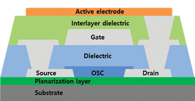
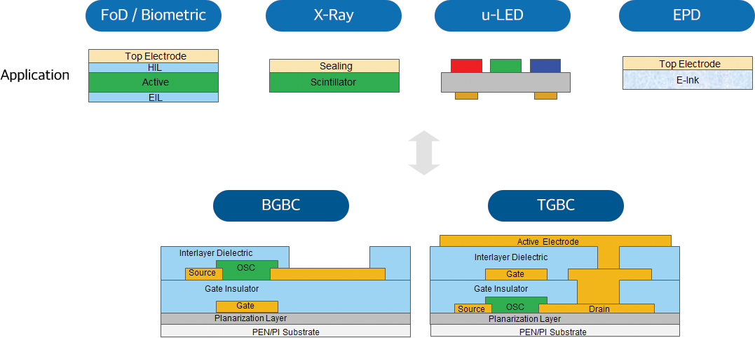
| OTFT Stacking Structure |  |
 |
 |
 |
 |
 |
 |
|
|---|---|---|---|---|---|---|---|---|
| Detail Process | Surface Treatment | S/D Electrode | OSC | Gate Insulator | Gate Electrode | Inter layer Dielectric | Cathode Electrode | |
| Organic material Coating | Spin | ○ | ○ | ○ | ○ | |||
| Slot Die / Inkjet | ○ | ○ | ○ | ○ | ||||
| PR Coating | Spin | ○ | ○ | ○ | ○ | ○ | ○ | |
| Slot Die | ○ | ○ | ○ | ○ | ○ | ○ | ||
| DFR | ○ | ○ | ○ | ○ | ○ | ○ | ||
| Electrode | Vacuum Deposition | ○ | ○ | ○ | ||||
| Electroless Plating | ○ | ○ | ○ | |||||
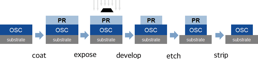
Specialties/Strengths
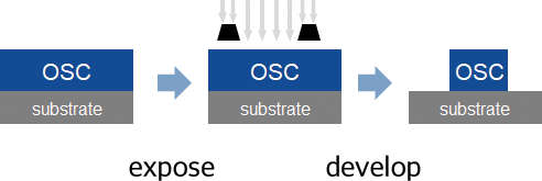
ㆍEliminate 3 Step (PR Coating, Etching, Strip)
ㆍNo need to use photoresist
ㆍCrosslinked material is not affected by subsequent processing
CLAP Co.,Ltd
1306 Ho, 1006, Cheonho-daero, Gangdong-gu, Seoul, Republic of Korea
CEO : Sungho, Kim / Business Registration Number_764-88-01246
Copyright (c) 2022 CLAP Co.,Ltd. All rights reserved.
E-mail_ johnny@clap.co.kr